Last month, a group of seven Florida A&M University (FAMU) students, four from the Electronic Engineering Technology program and three from Electrical Engineering, attended a transformative two-day semiconductor workshop at the University of Florida’s Nanoscale Research Facility (NRF). Led by Dr. Jack Judy, FSI Director of Workforce Development, Professor and Director of the Nanoscience Institute for Medical and Engineering Technologies (NIMET).
FAMU Students Gain Hands-On Semiconductor Training at UF’s Nanoscale Research Facility
Last month, a group of seven Florida A&M University (FAMU) students, four from the Electronic Engineering Technology program and three from Electrical Engineering, traveled to the University of Florida to participate in an intensive, hands-on two-day semiconductor workshop. This immersive experience took place at the University’s Nanoscale Research Facility (NRF) and was led by Dr. Jack Judy, FSI Director of Workforce Development, Professor, and Director of the Nanoscience Institute for Medical and Engineering Technologies (NIMET). The workshop was developed and managed by Dr. Judy in collaboration with UF Ph.D. candidate Kenneth Fluker, Dr. Brent Gila, and Andres Trucco, and was designed specifically for FAMU students to gain foundational and practical experience in microfabrication.
This training was part of a broader initiative supported by the National Science Foundation (NSF) under the grant “EAGER: Empowering African American STEM Talent: Enhancing Semiconductor and Microelectronics Expertise through Targeted Research and Mentorship at an HBCU,” led and co-led by Dr. Mulay and Dr. Chao Li, both professors at FAMU. Dr. Chao Li accompanied the FAMU students to the workshop and continues to support the program through mentorship and guidance.
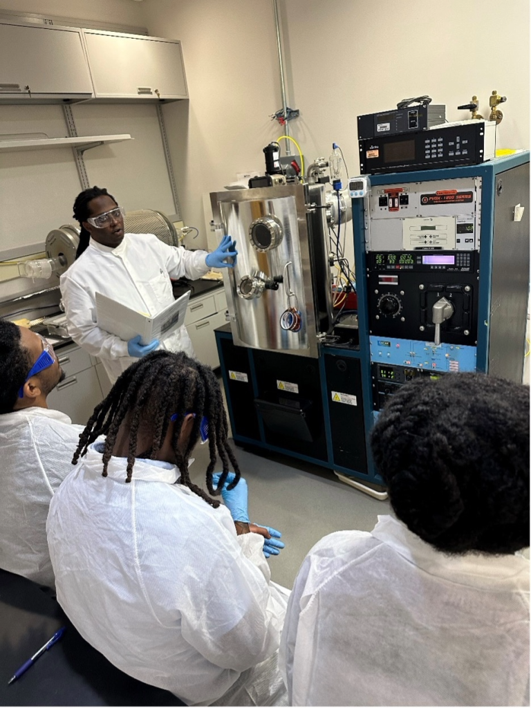
The workshop welcomed eight participants, seven students and one faculty member, and condensed what is typically a 15-week graduate-level course into an intensive two-day format. Dr. Judy personally welcomed the students, delivered several lectures each day to explain the theory behind semiconductor manufacturing, visited them in the lab to answer questions, and met with them individually at the conclusion of the course.
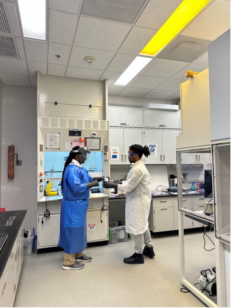
Hands-on lab sessions were at the heart of the experience. Kenneth Fluker, serving as the laboratory teaching assistant, worked side by side with the participants throughout both days inside the instructional microfabrication laboratory. Kenneth, a doctoral candidate nearing completion of his dissertation, is a graduate of Alabama State University, another HBCU. His expertise, clarity, and approachability played a vital role in helping students understand and execute each step of the complex fabrication process.
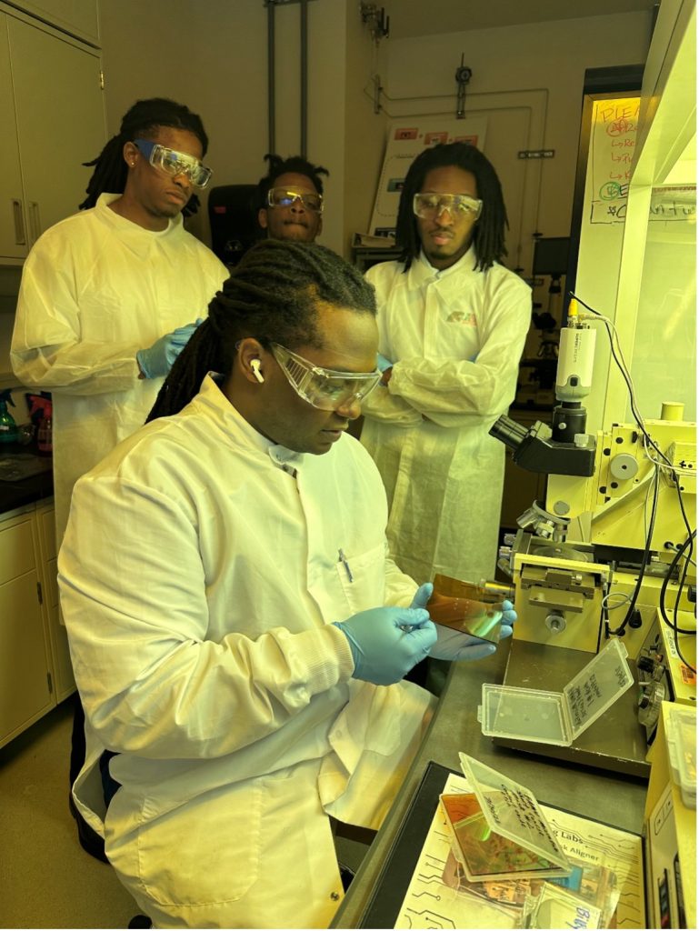
Dr. Brent Gila managed the NRF facility and ensured that everything ran smoothly behind the scenes, while Andreas Trucco supported the preparation and operation of all lab tools and equipment. Their roles were essential in delivering a seamless lab experience for the students. Together, the instructional team guided participants through a detailed 35-step process to fabricate and test their own silicon wafers with functional integrated microelectronic components, including MOSFETs and resistors.
Students handled advanced tools and materials, including hazardous chemicals such as hydrogen fluoride (HF), and high-temperature furnaces operating at 1000°C. Every student successfully fabricated and tested their own integrated circuit chip, and took it home as a memento of their achievement. But the impact of the experience reached far beyond the lab. It inspired new career interests and deepened appreciation for the semiconductor industry.
Ahmahd Denmark reflected on the experience: “Attending the two-day workshop at the University of Florida’s Nanoscale Research Facility was an incredibly rewarding and eye-opening experience. Under the guidance of Dr. Jack Judy and Kenneth Fluker, I gained a deeper understanding of the intricate steps involved in creating semiconductor devices. Their expertise, patience, and clear instruction made the learning process both approachable and engaging. Being able to not only learn the concepts but also work directly with the equipment gave me a true appreciation for the precision and attention to detail required in semiconductor fabrication. I left the workshop not only with new technical skills but also with a stronger appreciation for the role of nanoscale research in advancing technology. I’m already looking forward to returning for future training opportunities.”
Billy White added, “Taking part in the two-day Semiconductor Workshop at the University of Florida was a great learning experience for me. I got the chance to actually work in a cleanroom and use semiconductor fabrication tools, which was exciting since most of my learning before this had been from books or class. We went through important processes like etching, diffusion, and metrology, and it really helped me see how chips and devices are made step by step. The workshop gave me a better understanding of how the technology we use every day is built, and it made me even more motivated to keep learning and applying these skills in Computer Engineering.”
Ultimately, the workshop proved to be more than just an academic experience. It served as a launching pad for future research, advanced study, and professional growth. Through collaborative mentorship, NSF support, and outstanding instruction, this initiative is helping to cultivate the next generation of engineers and researchers in the semiconductor industry.