Semiconductor Manufacturing in Florida: Power. Progress. Possibilities.
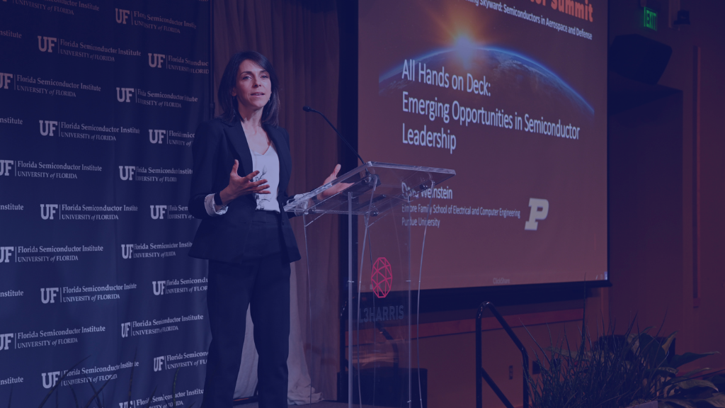
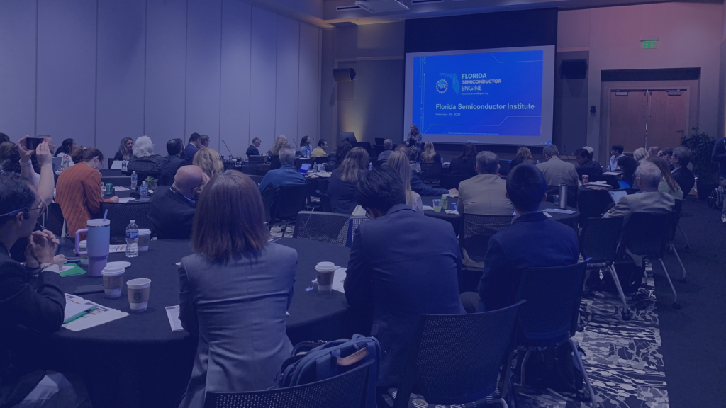
Presentation Recap
Mark Your Calendars!
You’re invited to the 2026 Florida Semiconductor Summit! From February 23rd – 25th, 2026, the Florida Semiconductor Institute is hosting the fourth annual Florida Semiconductor Summit at the Rosen Shingle Creek. This year’s summit theme is “Semiconductor Manufacturing in Florida: Power. Progress. Possibilities.” This summit offers a unique opportunity to connect with industry leaders, explore cutting-edge advancements, and delve into the evolving role of semiconductor manufacturing in the state of Florida.
What Makes this Year’s Summit the Biggest Yet?
This year, we are taking the summit to the next level! Not only are we bringing together industry leaders from top CEOs to leading academics, we are bringing together rising startups and industry pioneers who are shaping the future of semiconductor technology in our first ever interactive exposition hall. This is your chance to connect with key decision-makers, gain insights from cutting-edge research, and explore new business opportunities in one of Florida’s fastest-growing sectors. The summit offers invaluable networking, knowledge-sharing, and a front-row seat to innovations that will have deep impacts on the state of Florida. Don’t miss out, register today!
Date
Feb. 23-25, 2026
Thank You to Our Event Partners
Save Your Spot for the 2026 Florida Semiconductor Summit
Register today, as space is limited!
Location
Rosen Shingle Creek Orlando
Located just 10 minutes away from the Orlando International Airport and around the corner from Orlando’s premiere attractions, Rosen Shingle Creek Orlando is in a prime location for experiencing Orlando. The natural beauty and manicured fairway of the Shingle Creek Golf course and Shingle Creek, the head of the Everglades, offers guests a serene, calming environment that you won’t forget.
Program Highlights
Check back soon for the full Summit program. For now, check out our program highlights and new additions below.
Exposition Hall
New for 2026
Learn More
Innovation Pitch Competition
New for 2026
Learn More
Chip Chats
New for 2026
Learn More
Keynote Speakers
Breakout Sessions
Networking
Keynote Speakers

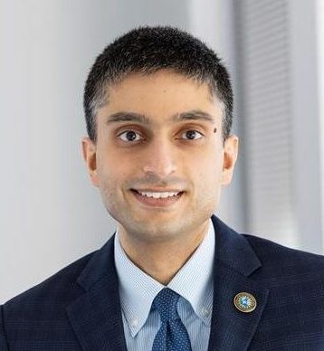
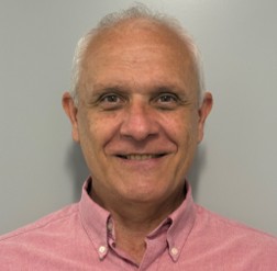
Thomas Sonderman
CEO, SkyWater Technology
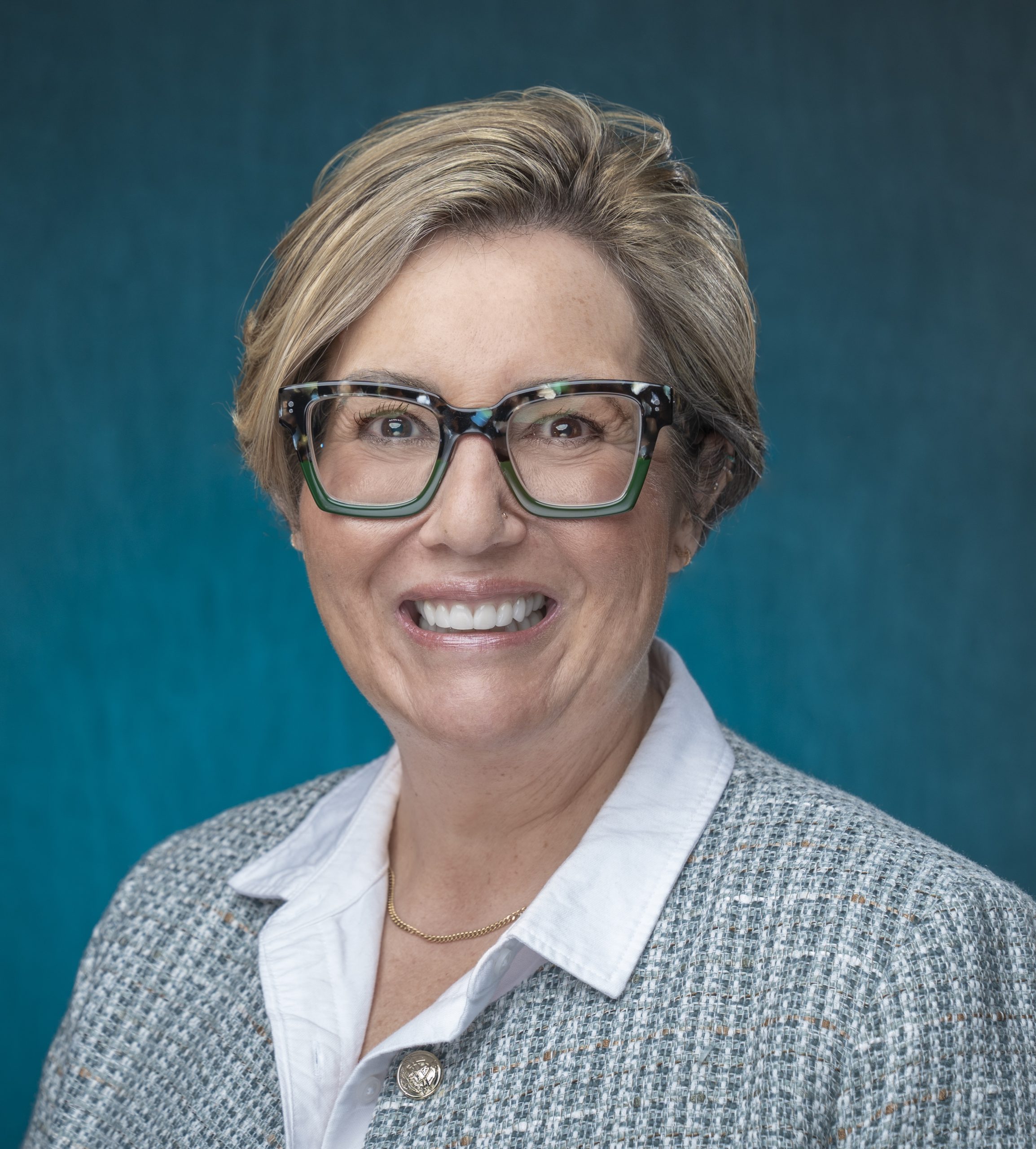
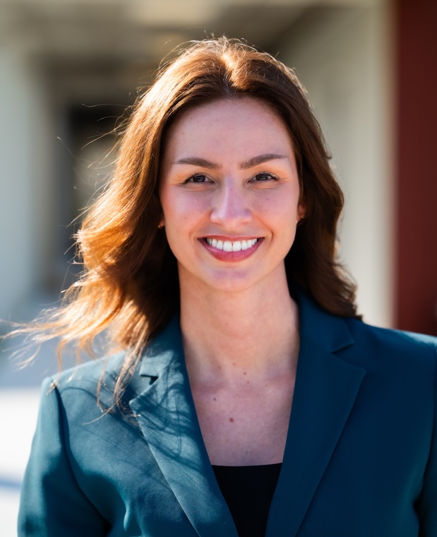
Michelle Williams
Executive Director, SEMI Foundation

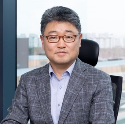
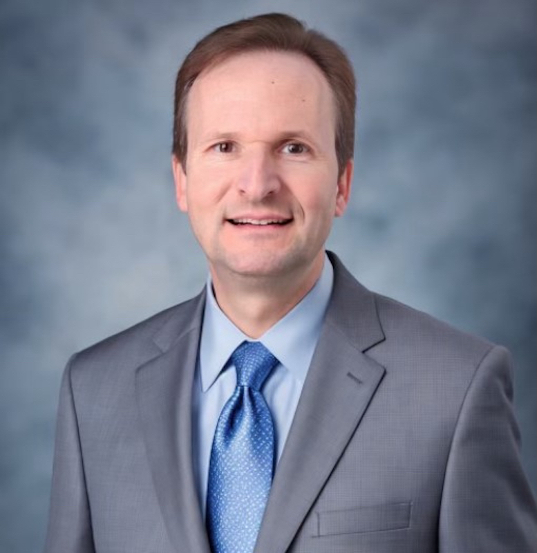
Dr. Woong-Sun Lee
CEO, SK hynix West Lafayette
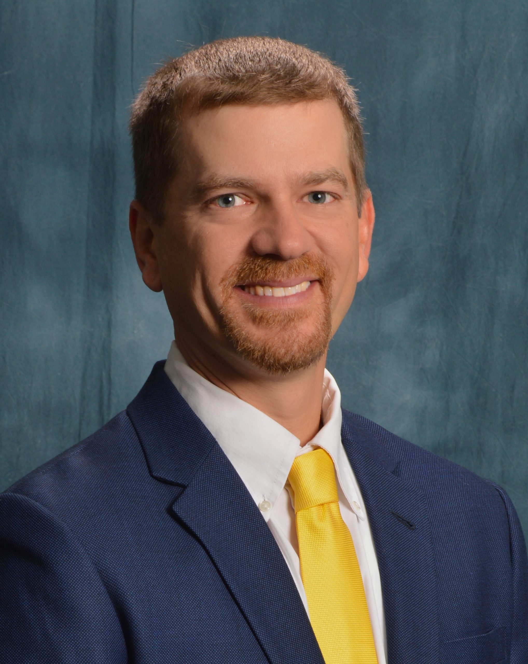
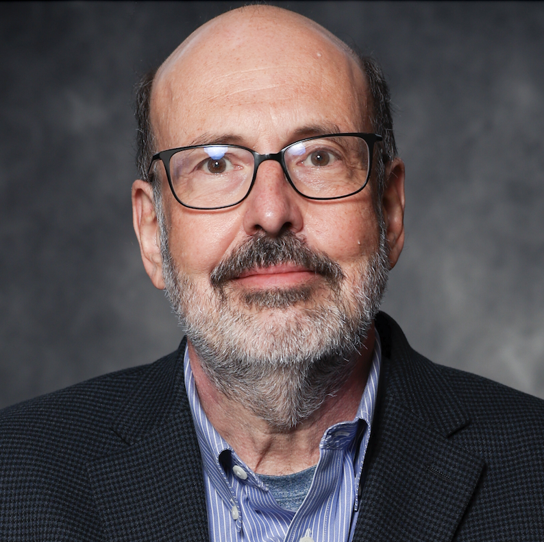
Dr. Erwin Gianchandani
Assistant Director TIP Directorate, National Science Foundation

Dr. Mark Lundstrom
Don and Carol Scifres Distinguished Professor of Electrical and Computer Engineering, Purdue University
Invited Speakers


Summit Agenda
Subject to Change
Link to Program Book: https://fsi.institute.ufl.edu/2026-florida-semiconductor-summit-program-book/
Summit Chairs
Thank you to our Summit Chairs that help make Florida Semiconductor Summit possible!
Dr. Gloria Kim
University of Florida, FSI Assistant Director of Partnerships, Assistant Professor

Dr. John Volakis
Florida International University, Professor
Our Sponsors
Interested in sponsoring this event to support, inspire, and advance the industry?
Platinum
Gold

Silver

Media Sponsor
Refreshment Breaks Sponsor
Exhibitors
AltaScient LLC
Bluegrass Educational Technologies
Florida Semiconductor Institute
IC2
imec
Mattrix Technologies
MMEC
NSF I-Corps | UF Innovate Pathways
P.K. Yonge Developmental Research School, University of Florida, FIRST Robotics Team 4118 & Steel Eel Robotics FTC 18317
Rigaku Americas
Rohde & Schwarz
Trion Technology, Inc.
University of Central Florida
University of South Florida
Workforce Development Posters
| Name of Authors | University | Poster/Abstract Title | Abstract |
| Markondeya Raj Pulugurtha, John Volakis, Mst Shahim Ara Shawkat, Satheesh B Venkatakrishnan and Vladimir Pozdin | Florida International University | Hands-On Semiconductor Design and Electronics Systems Manufacturing Read the full abstract here | The Hands-On Semiconductor Design and Electronics Systems Manufacturing program provides students with immersive, laboratory-centered training across the full spectrum of semiconductor device fabrication and electronic system development. Students gain direct experience with state-of-the-art nanofabrication tools, including advanced lithography, chemical and physical vapor deposition techniques, and precision etching processes essential for modern semiconductor manufacturing. Complementing this fabrication focus, an integrated sequence of courses covers RF design principles, high-frequency circuit implementation, and system-level integration. Students are also introduced to the fundamentals of integrated circuit (IC) design, building a strong foundation in device architecture, layout, and performance optimization. A dedicated curriculum track further explores sensor materials, signal processing devices, and system integration strategies tailored for wearable medical technologies. By combining hands-on fabrication, circuit design, and application-driven system integration, the program prepares students to innovate across semiconductor manufacturing, RF systems, and next-generation biomedical electronics. |
| Markondeya Raj Pulugurtha, John Volakis, Satheesh B Venkatakrishnan and Vladimir Pozdin | Florida International University | Semiconductor Packaging Courses at FIU | We offer comprehensive courses in semiconductor packaging that equips students with both foundational knowledge and advanced technical expertise in modern hardware integration. The curriculum covers the evolution of semiconductor hardware, heterogeneous integration using 3D packaging and interposer technologies, advanced substrate fabrication processes, and next-generation assembly methodologies. Students engage in in-depth electrical, mechanical, and materials process analyses, applying multidisciplinary engineering principles to real-world applications. The course emphasizes reliability assessment and failure modeling, enabling students to evaluate performance trade-offs and design constraints. As a culminating experience, each student conducts a detailed technical study of a selected product within the biomedical sensor, communications, or computing markets. This program prepares students to address the complex challenges of advanced semiconductor packaging and to contribute effectively to next-generation system integration and product innovation. |
| John Zulugaga, Leo Elhaouji | University of Central Florida | Semiconductor Education and Readiness Pathway at UCF | To meet the growing workforce demand in semiconductor manufacturing, the University of Central Florida (UCF) has developed an integrated Semiconductor Education and Readiness Pathway combining curriculum innovation, cleanroom-based training, and industry engagement. This initiative includes new undergraduate courses in semiconductor manufacturing, materials, thin film technology, and device fabrication, along with a structured 2+2 AS–BS pathway in Semiconductor Engineering Technology. A key component is the SMART (Semiconductor Manufacturing and Advances in Recent Technologies) two-week intensive summer workshop, offering hands-on training in cleanroom safety, deposition, lithography, etching, and device fabrication. Delivered in 2024 and 2025, SMART bridges academic learning with real-world fabrication experience. Together, these efforts create a scalable model for building a skilled semiconductor workforce. |
| Christian Turner, Arianna Balsamo | University of Central Florida | UCF Cleanroom to Career (C2C) Pipeline for Hands-On Semiconductor Career Preparation | The UCF Department of Electrical and Computer Engineering has launched the Cleanroom to Career (C2C) pipeline—an innovative pathway that builds strong foundational knowledge by enabling hands-on learning, gain real-world fabrication experience, and comprehensive cleanroom training to prepare students for semiconductor industry careers. |
| Jack W. Judy, Erin Patrick, and Tan Wong | University of Florida | UF Courses that Provide Training for Careers in the Semiconductor Industry | The Herbert Wertheim College of Engineering at the University of Florida provides a wide range of courses spanning multiple departments that train undergraduate and graduate students for careers in the semiconductor industry. This poster summarizes the broad array of courses by organizing them into technical topic areas. We are also in process of offering Florida Semiconductor Institute Recognitions (digital certificates) to students that complete industry-selected sets of courses on topics of greatest need by different sectors of the industry. The faculty welcome the input from industry regarding suggestions on how to expand and/or refine our course offerings to take into account current industry needs and professional realities. If you have suggestions or are willing to identify course groupings for industry-driven FSI Recognitions, please contact Prof. Jack Judy (cell: 352-672-1787). |
| Kenneth Fluker, James Overmeyer, Andreas Trucco, Brent Gila, and Jack W. Judy | University of Florida | UF Semiconductor Device Fabrication Laboratory Course | The University of Florida (UF) has offered one or more hands-on laboratory courses focused on semiconductor device fabrication, materials, and/or chemical processes, since the 1970s. Currently the UF Electrical and Computer Engineering (ECE) Department enrolls ~30 students each semester in EEE 5354L: Semiconductor Device Fabrication Laboratory. Since 2013, this course has trained over 700 students. In this hands-on laboratory course, the students use fabrication and metrology tools and test and measurement equipment in two instructional labs managed by the Nanoscale Research Facility (NRF) staff. The students work in pairs to complete a microfabrication process that yields an array of MOSFETs, diodes, resistors, and test structures that they characterize. This practical laboratory course is designed to complement courses focused on microfabrication theory. During the summer we have provided a condensed 2-to-3-day version of the lab experience for students from Florida A&M University, which is an instate HBCU that lacks the facilities to offer such a learning experience. The eight FAMU students that participated in the 2025 summer short course really liked it a lot. Seeking Corporate Sponsors: Although the equipment dedicated for this lab course is maintained well by the NRF staff, some of the key equipment is very old and increasingly hard to maintain. In addition, there is a need to add more test-and-measurement equipment (e.g., parameter analyzers, probe stations, micromanipulators, etc.) to expand the number of testing stations to improve the student experience and knowledge gain. If your company is willing to sponsor the lab through a financial or equipment donation, please contact Prof. Jack Judy (cell: 352-672-1787). |
| John Taylor Maurer, Isabelle Eskanos, Kaleb Sharrer, Marcelo Farfan, Peter Kveton, Ahmed Mamdouh Mohamed Ahmed, Samuel Zucker, Justin Mcmillen, Fawaz Razak, Harshen Patel, Phaneshwar Dundigalla, Chanyapat Sriviroch, Samir Ahmed, Muhammad Shahbaz Rafique | University of South Florida | USF NRT Microelectronics Fabrication Lab PMOS Metal Gate Process | For the Spring 2025 semester of this laboratory course, we were tasked with undergoing a 10-micron p-type metal-oxide semiconductor (pMOS) Metal Gate process (Figure 1) to fabricate a layout design on silicon wafers with the Nanotechnology Research & Education Center (NREC) facility at the University of South Florida (USF) Tampa Campus. Throughout the course, we were trained in lab safety, equipment usage, and process operations within the NREC cleanroom. Additionally, we collected metrology data to assist the NREC facility in characterizing their process |
Social Media Kit
Share your involvement in the 2026 Florida Semiconductor Summit (FSS)!
Download official event graphics to announce your participation and help spread the word. Each section includes pre-sized graphics and suggested captions to make posting easy and professional.
FAQ
The 2026 Summit will be held at the Rosen Shingle Creek, located in Orlando FL, from February 23-25.
The summit welcomes professionals, researchers, educators, startups, and students involved or interested in Florida’s growing semiconductor ecosystem.
You can register for the event here: Register Here
The deadline for early registration is January 11th, 2026. The registration fee will rise to $275 starting on January 12th.
Yes, discounted room rates will be available for attendees staying at the host hotel and nearby partner properties. More information can be found on the location page:
The exhibit hall will showcase leading semiconductor companies, university research centers, startups, and workforce organizations. Attendees will have the opportunity to explore cutting-edge technologies, learn about new initiatives, and connect directly with exhibitors driving semiconductor innovation in Florida and beyond.
Exhibitors will include a mix of industry leaders, academic institutions, government partners, and emerging startups across the semiconductor supply chain. A full list of exhibitors will be available closer to the event date.
Yes, lunch and refreshments will be provided during scheduled breaks.
Yes, on-site parking will be available at the hotel for a discount of 50% off the daily rate.
Sessions will explore semiconductor manufacturing, materials, advanced packaging, workforce development, R&D collaborations, and public–private partnerships advancing Florida’s semiconductor strategy.
Presentation materials may be available to registered attendees after the summit, pending speaker approval.
Information about sponsorship and exhibition opportunities is available in the Sponsorship Prospectus. To register as a sponsor or exhibitor, please visit the Registration Page and select “Sponsor/Exhibitor” as your registration type.
If you’re unable to attend, please email fsi-info@ufl.edu as soon as possible. In order to receive a full refund, cancellations must be received via email on or before January 16, 2026. A 50% refund will be issued for cancellations received between January 17 – February 6, 2026. No refunds will be available after February 6th, 2026 due to event commitments.
Yes, substitutions are welcome. If you are unable to attend, you may transfer your registration to a colleague at no additional cost up until February 6, 2026. Please notify us of this transfer via email and provide us with your colleague’s first and last name, as well as the organization they are from and their email address. This information will be used to create their name badge.
For general inquiries, please contact fsi-info@ufl.edu.
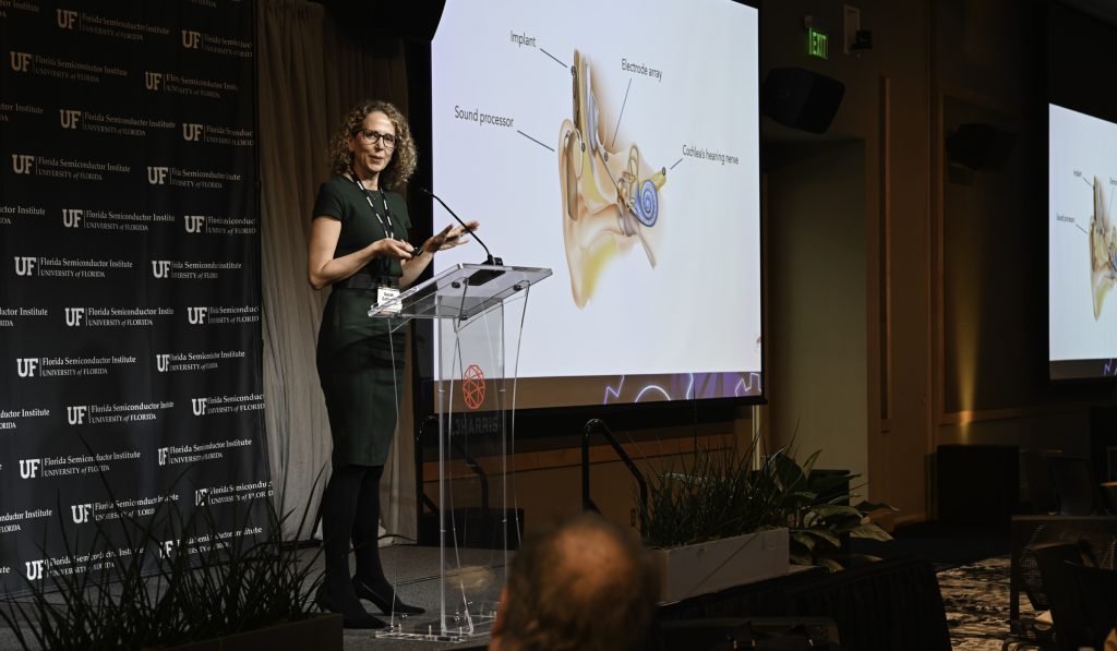
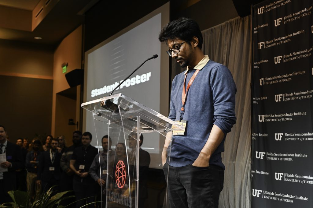
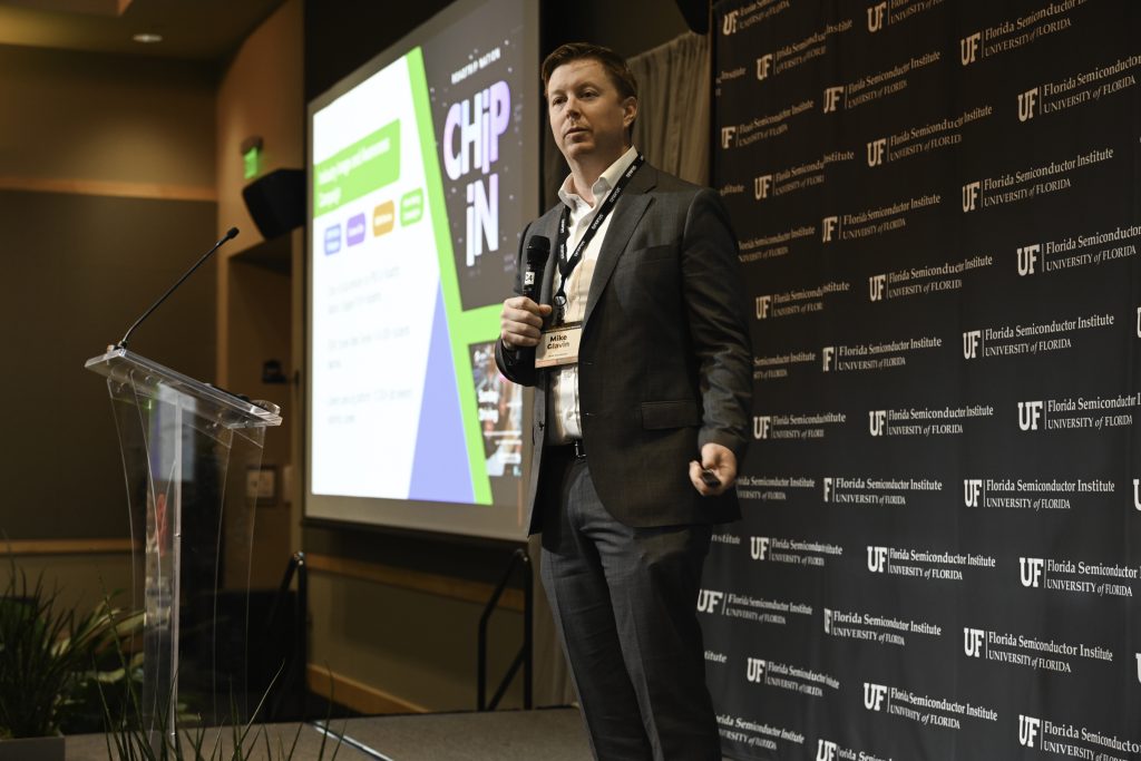
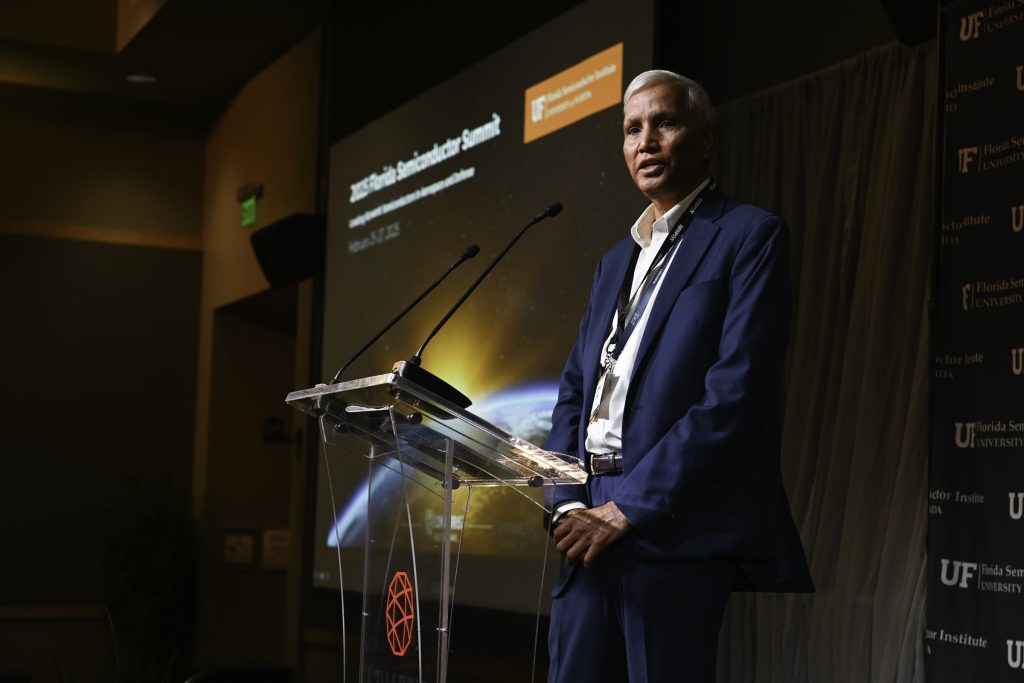
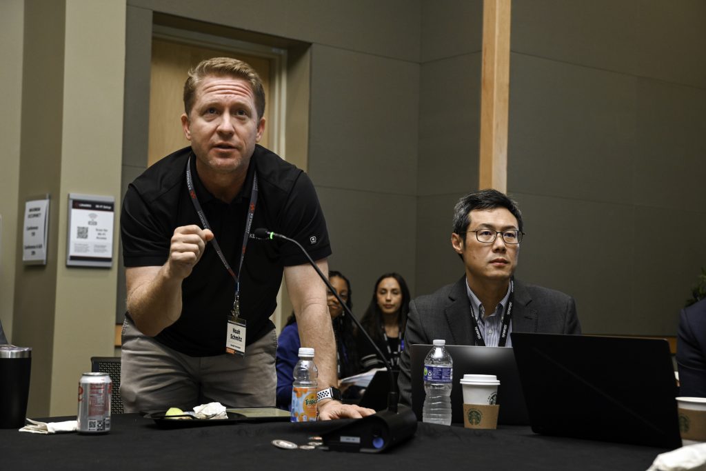
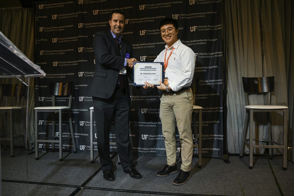
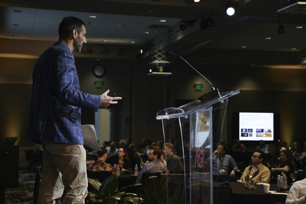
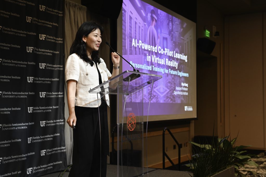
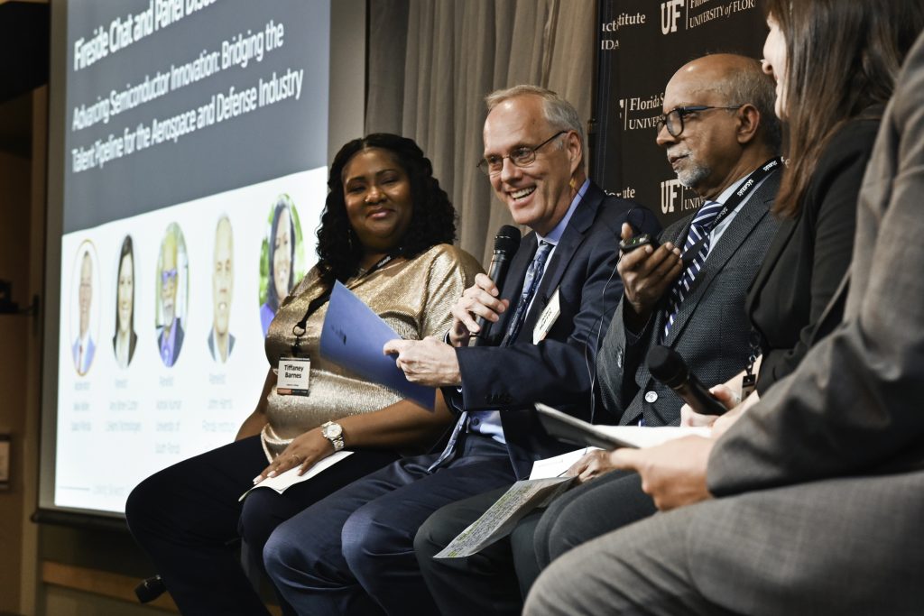
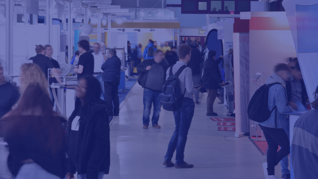
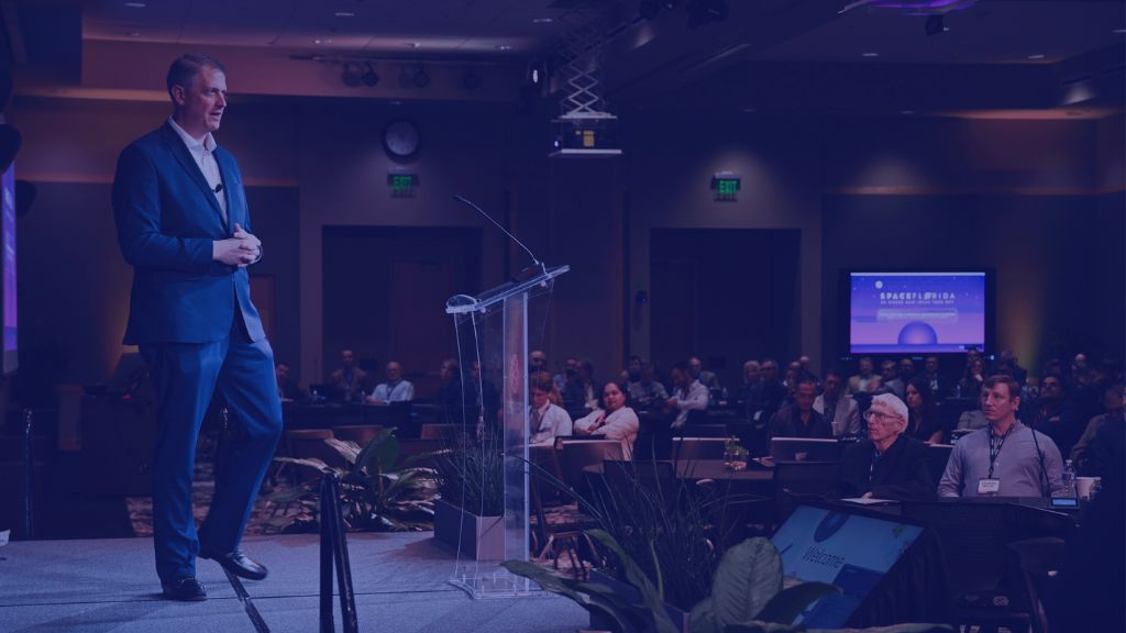
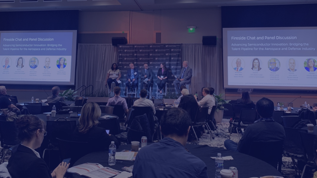
2025 Photo Gallery